Introduction
Read Consulting failure analysis laboratory was asked to perform an electronic failure analysis to determine the root cause failure mode of surface mount glass encapsulated Zener diodes . For this study, the client submitted 4 failed Zener diodes and 12 unused Zener diodes.
Preliminary Conclusion
The root cause of the failures is cracking of the glass envelope due to interference of the glass envelope with the metal ends of these Zener diodes. The resulting cracking at the ends causes the ultimate failure. All indications are that the present diodes are flawed in the as received condition, and they are going to cause high yield losses in assembly. There may be a contribution from mounting stresses, but it is believed that these are secondary to the major cracking problems with the as received diodes.
Strategy
The strategy is to perform failure analysis on cracked diodes submitted. Use these results to determine the root cause of the failures. This includes examining new diodes from the same factory and to look at similar diodes made elsewhere.
Part Description
These parts (Figure #1) are surface mount, glass encapsulated Zener diodes that measure a forward bias resistance of approximately 12.2 ohms. These parts have an outer diameter of 0.094” and an overall length of 0.192”. The silicon Zener diode is cemented to two copper rods. All of this is encapsulated inside a glass tube. Essentially, there three materials involved in this assembly with distinct coefficients of thermal expansion (Cu 16.5ppm, Soda Lime Glass 8.6ppm and Silicon 2.6ppm). This Zener diode is solder mounted on a printed circuit board that has a coefficient of thermal expansion of 14ppm. It is important to note that this is a rigid system with no visible strain relief. Therefore, differences in thermal expansion can be critical.
Procedure
Four failed diodes were examined microscopically to perform the root cause failure analysis. In addition, new diodes and a commercial standard mount Zener diode (i.e. intended for through the board mounting) were also examined optically and with an optical microscope.
Part Description
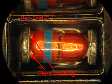
Figure #1: Photomicrograph of an as received glass encapsulated diode. These parts have an outer diameter of 0.094” and an overall length of 0.192”. The silicon diode is situated between what appears to be two copper rods. All of this is encapsulated inside a glass tube. Essentially, there three materials involved in this assembly with distinct coefficients of thermal expansion (Cu 16.5ppm, Soda Lime Glass 806ppm and Silicon 2.6ppm) (Mag. 10X).
 |
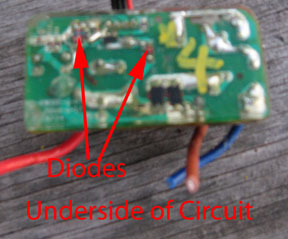 |
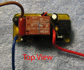
Figure #2: Photographs of a representative control board. The diodes in question are on the underside of the board and they are encapsulated in rigid polyurethane.
 |
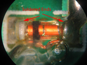 |
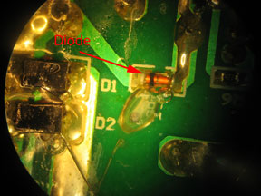
Figure #3: Photomicrographs of a diode on a representative control board. The diodes in question are on the underside of the board and they are encapsulated in rigid polyurethane. It is important to note that there is no strain relief for the glass encapsulated diode.
Discussion
It appears that the Zener diodes assembled onto the printed circuit boards are inconsistent in quality. In addition, there is cracking associated with the metal end contacts. Observations indicate that the glass envelopes of the present diodes are cracked when received, and they are going to cause high yield losses in assembly. Below is a list of questions arising from this work:
- Is it possible to successfully surface mount glass encapsulated Zener diodes on a printed circuit board?
- If the entire circuit is encapsulated, are glass sealed diodes necessary?
- Strain relief would occur automatically if through the board devices were used.
- Yield losses will be high if these devices are manually assembled onto the printed circuit board.
Results
Failed Parts
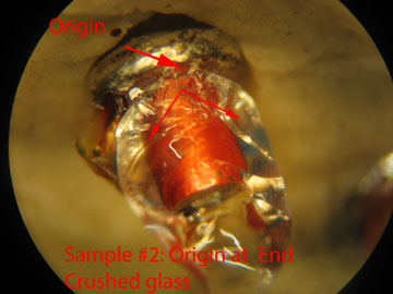
Figure #4: Photomicrograph of failed sample #2. The glass failure initiated at a “crush point” where the glass and a large “blob” of solder are in contact. Also, it appears that there is encapsulant material on the glass fracture surface. This indicates that this diode was cracked before encapsulation in polyurethane (Mag. 10X).
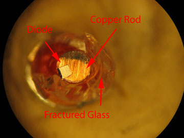
Figure #5: View of the diode still attached to one of the copper rods. Direct electrical measurements on the diode show the correct forward resistance. So this diode was still electrically connected to one of the copper rods. It is believed that the diode is attached with a conductive cement (Mag. 8X).
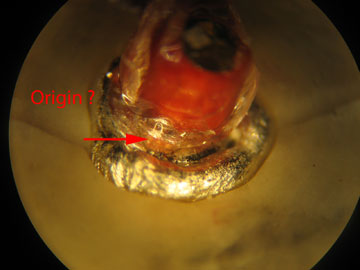
Figure #6: Photomicrograph of failed sample #4. Again, direct electrical measurements on the diode show the correct forward resistance. So this diode was still electrically connected to one of the copper rods. The glass failure initiated at a “crush point” where the glass and a large “blob” of solder are in contact. (Mag. 10X).
Figure #7: Photomicrograph of failed sample #7. Again direct electrical measurements on the diode show the correct forward resistance. So this diode was still electrically connected to one of the copper rods. This failure was difficult to analyze; however, it is believed that glass failure initiated at a “crush point” where the glass and a large “blob” of solder are in contact. (Mag. 12X).
Examination of Unused Diodes

Figure #8: Photomicrograph of an as received surface mount glass encapsulated diode. Close examination of one end shows cracking. Essentially, there three materials involved in this assembly with distinct coefficients of thermal expansion (Cu 16.5ppm, Soda Lime Glass 806ppm and Silicon 2.6ppm). There is cracking at one end. Later these cracks could initiate failure of the glass envelope. This is consistent with the failure analysis results (Mag. 10X).
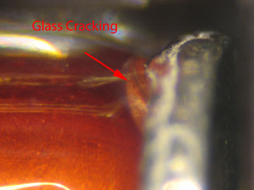
Figure #9: Close up photomicrograph of the cracking (Mag. 50X)
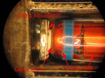
Figure #10: Photomicrograph of what is believed to be a good end of an as received glass encapsulated diode. It appears as if there is some sort of glass bead seal/shock absorber. (Mag. 10X).
Standard Mount Glass Encapsulated Zener Diode
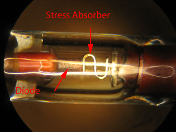
Figure #11: Off the shelf standard mount (Through the board) glass encapsulated Zener diode. Inside there is an ‘S’ shaped contact. Presumably, this is there to relieve stress. In addition, there is strain relief through the wire leads.
 |
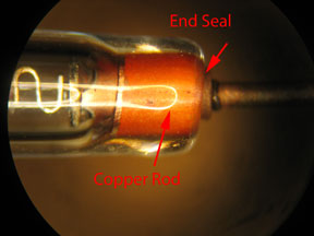 |
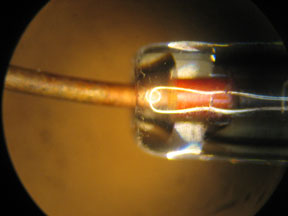
Figure #12: Photomicrographs of the ends of the Zener diode shown in Figure #9. Granted this is not a surface mount device; however, one can see the end seals are much better.


